W200 Power Amplifier
A fully discrete complementary Class-AB power amplifier using matched small-signal stages and TIP35C / TIP36C bipolar output devices.
Overview
The W200 is a fully discrete complementary Class-AB power amplifier developed as part of the Ward Audio amplifier project work. The design uses TIP35C and TIP36C bipolar output devices, a discrete small-signal front end, active current-mirror stages, adjustable bias, discrete drivers, and a complementary emitter-follower output stage.
The W200 is intended as a power-amplifier module rather than a complete stand-alone amplifier. Over-current and loudspeaker protection are deliberately handled externally, allowing the amplifier to be paired with a dedicated amplifier output controller or speaker-protection module appropriate to the final installation.
Matched Small-Signal Stages
The differential input devices and current-mirror devices are implemented using matched transistors from OnSemi. This provides substantially better device matching and thermal tracking than can normally be achieved with individually packaged discrete transistors.
Because the paired devices share the same silicon and closely track one another in temperature, parameters such as base-emitter voltage remain closely matched as operating temperature changes. In the differential stages this helps reduce input imbalance and DC offset drift, while in the current mirrors it improves current matching and symmetry between the corresponding signal paths.
The practical benefits include improved thermal tracking, better current-mirror accuracy, reduced sensitivity to individual transistor variation, improved channel-to-channel repeatability, and reduced distortion caused by small-signal device mismatch.
Bipolar electrolytic capacitors in the signal path are selected from Nichicon's MUSE audio series. These capacitors are used where a non-polar electrolytic is appropriate, allowing AC signal coupling without imposing a fixed polarity across the capacitor.
Circuit Topology
The W200 uses a complementary discrete signal path built around matched differential and current-mirror stages, followed by a discrete voltage-amplification stage, adjustable bias network, complementary driver stage, and bipolar power output stage.
Matched PNP/NPN devices are used where device tracking has the greatest influence on small-signal behavior. The output section uses Toshiba's TTC004B/TTA004B complementary drivers feeding ST Micro's complementary TIP35C and TIP36C power transistors.
The amplifier also includes local supply decoupling and an output stability network consisting of an output inductor/resistor network and Zobel compensation.
Output Stage
The standard W200 configuration uses twp pairs complementary TIP35C and TIP36C bipolar power transistors. The power devices mount on the underside of the PCB, allowing them to bolt directly to the amplifier heatsink while the PCB mounts directly above them.
This arrangement keeps the high-current output connections short, simplifies mechanical assembly, and allows the PCB and output devices to form a compact amplifier module around the heatsink.
The W200 architecture is not limited to a single output-device arrangement. Other output-stage configurations and device complements can be used where different supply voltages, output-power requirements, thermal requirements, or load conditions call for them.
Protection Architecture
The W200 does not include an onboard over-current limiter or loudspeaker disconnect circuit. This is intentional.
The amplifier is designed to operate with an external amplifier output controller or speaker-protection system. Separating these functions keeps the amplifier signal path independent of the protection hardware and allows protection behavior to be selected for the requirements of the finished amplifier.
An external protection controller can provide functions such as DC-fault detection, output-current monitoring, startup and shutdown sequencing, loudspeaker connection control, and fault recovery without requiring those functions to be built directly into the W200 amplifier board.
Measurements
Approximately 90 W into 6.5 Ω at 12 kHz, immediately below clipping.
THD+N approximately -87 dB.
These are development-stage measurements rather than final published specifications. Additional characterization across frequency, output power, load impedance, noise, distortion, and clipping behavior will be added as testing continues.
PCB and Mechanical Design
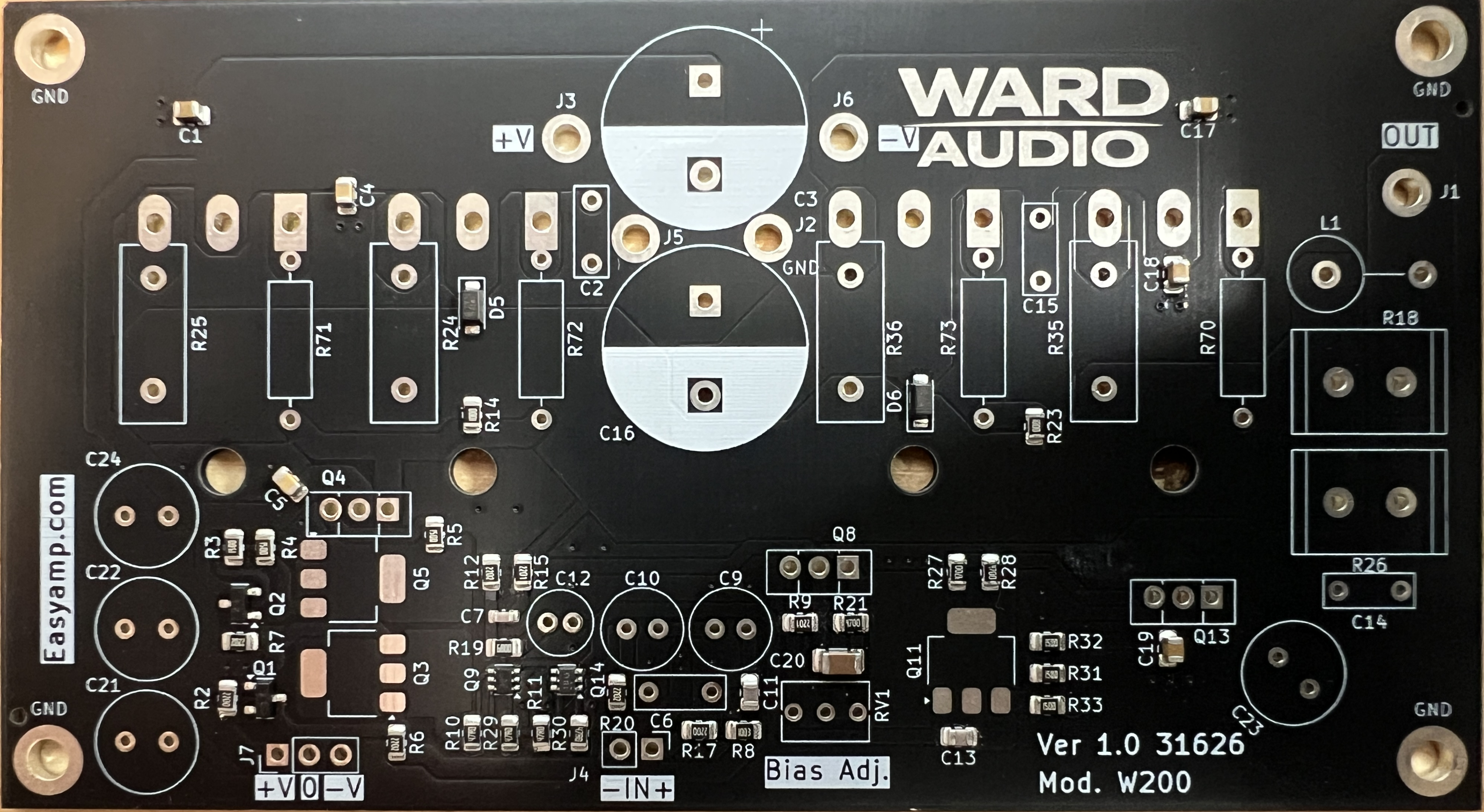
The W200 is built around a dedicated amplifier PCB containing the complete small-signal, bias, driver, supply-decoupling, and output-network circuitry.
The output transistors are installed beneath the PCB and mount directly to the heatsink. This keeps the power stage mechanically compact while minimizing the length of the high-current connections between the driver circuitry, output devices, supply rails, and amplifier output.
The board shown here is W200 Version 1.0 and represents the current hardware development platform.